PCB Library Administration done by Fortitude Tech
Design engineer spends a lot of time creating and maintaining schematic symbols and PCB footprint libraries.
The component cannot be placed on the circuit causes delay in project as pCB library is not available which
incurring additional cost.
This process is very time consuming, error prone and causes delay to design a product. Leave the PCB library
building to us, then you can get on with the important engineering stuff.
Our PCB Library experts let you effortlessly calculate and generate high quality footprints in a fraction of time.
Drawing a schematic circuit diagram is the most crucial step of PCB design and should never be compromised or overlooked. For that you need a designing software such as Eagle, Diptrace, Allegro, Altium or Pads software.
After the completion and simulation of the circuit the schematic capture is contained within a file and is converted into a format which is called netlist. It contains all the tiny but crucial information such as circuit nodes, component pins and the respective pin connections. Thus the PCB is designed keeping the width, board edge spacing, hole spacing, trace sizes under consideration.
The next step involves the printing the PCB of the schematic design producing the desired output. Manufactures performs DFM checks on the circuit and then finalize it to generate a film from circuit board diagram of the PCB layout software.
PCB Design Service
How does our PCB Design Service work?
1. PCB Design of single layer, two layer, multi-layer, rigid, Flex, rigid-flex PCBs.
2. Highly complex & dense PCB designs done with ease.
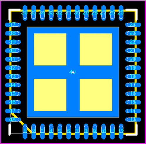
3. Advanced component footprints & library creation including BGA, QFN packages.
4. PCB reverse engineering service
5. Re-engineering services to correct flaws or to optimize existing PCB designs for lowering costs
6. Testing services of PCB design
7. PCB Prototyping
Our Prestigious clients
we design products for the following customers